
PN Junction Diode
A PN-junction diode is formed when a p-type semiconductor is fused to an n-type semiconductor creating a potential barrier voltage across the diode junction The effect described in the previous tutorial is achieved without any external voltage being applied to the actual PN junction resulting in the junction being in a state of equilibrium. However, if we were to make electrical connections at the ends of both the N-type and the P-type materials and then connect them to a battery source, an additional energy source now exists to overcome the potential barrier.
The effect of adding this additional energy source results in the free electrons being able to cross the depletion region from one side to the other. The behaviour of the PN junction with regards to the potential barrier’s width produces an asymmetrical conducting two terminal device, better known as the PN Junction Diode.
A PN Junction Diode is one of the simplest semiconductor devices around, and which has the characteristic of passing current in only one direction only. However, unlike a resistor, a diode does not behave linearly with respect to the applied voltage as the diode has an exponential current-voltage ( I-V ) relationship and therefore we can not described its operation by simply using an equation such as Ohm’s law.
If a suitable positive voltage (forward bias) is applied between the two ends of the PN junction, it can supply free electrons and holes with the extra energy they require to cross the junction as the width of the depletion layer around the PN junction is decreased.
By applying a negative voltage (reverse bias) results in the free charges being pulled away from the junction resulting in the depletion layer width being increased. This has the effect of increasing or decreasing the effective resistance of the junction itself allowing or blocking current flow through the diode.
Then the depletion layer widens with an increase in the application of a reverse voltage and narrows with an increase in the application of a forward voltage. This is due to the differences in the electrical properties on the two sides of the PN junction resulting in physical changes taking place. One of the results produces rectification as seen in the PN junction diodes static I-V (current-voltage) characteristics.
There are two operating regions and three possible “biasing” conditions for the standard Junction Diode and these are:
- Zero Bias – No external voltage potential is applied to the PN junction diode.
- Reverse Bias – The voltage potential is connected negative, (-ve) to the P-type material and positive, (+ve) to the N-type material across the diode which has the effect of Increasing the PN junction diode’s width.
- Forward Bias – The voltage potential is connected positive, (+ve) to the P-type material and negative, (-ve) to the N-type material across the diode which has the effect of Decreasing the PN junction diodes width.
Zero Biased Junction Diode
When a diode is connected in a Zero Bias condition, no external potential energy is applied to the PN junction. However if the diodes terminals are shorted together, a few holes (majority carriers) in the P-type material with enough energy to overcome the potential barrier will move across the junction against this barrier potential. This is known as the “Forward Current” and is referenced as IF Likewise, holes generated in the N-type material (minority carriers), find this situation favourable and move across the junction in the opposite direction. This is known as the “Reverse Current” and is referenced as IR. This transfer of electrons and holes back and forth across the PN junction is known as diffusion, as shown below:
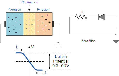
The potential barrier that now exists discourages the diffusion of any more majority carriers across the junction. However, the potential barrier helps minority carriers (few free electrons in the P-region and few holes in the N-region) to drift across the junction. Then an “Equilibrium” or balance will be established when the majority carriers are equal and both moving in opposite directions, so that the net result is zero current flowing in the circuit. When this occurs the junction is said to be in a state of “Dynamic Equilibrium“. The minority carriers are constantly generated due to thermal energy so this state of equilibrium can be broken by raising the temperature of the PN junction causing an increase in the generation of minority carriers, thereby resulting in an increase in leakage current but an electric current cannot flow since no circuit has been connected to the PN junction.
Reverse Biased PN Junction Diode
When a diode is connected in a Reverse Bias condition, a positive voltage is applied to the N-type material and a negative voltage is applied to the P-type material. The positive voltage applied to the N-type material attracts electrons towards the positive electrode and away from the junction, while the holes in the P-type end are also attracted away from the junction towards the negative electrode. The net result is that the depletion layer grows wider due to a lack of electrons and holes and presents a high impedance path, almost an insulator. The result is that a high potential barrier is created thus preventing current from flowing through the semiconductor material.
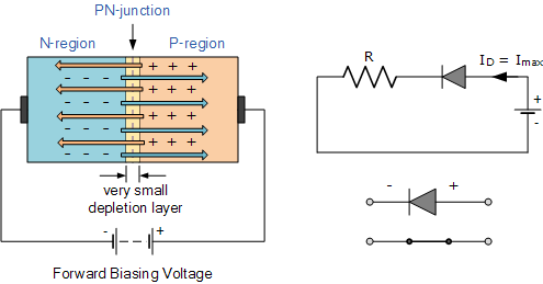
Forward Biased PN Junction Diode
When a diode is connected in a Forward Bias condition, a negative voltage is applied to the N-type material and a positive voltage is applied to the P-type material. If this external voltage becomes greater than the value of the potential barrier, approx. 0.7 volts for silicon and 0.3 volts for germanium, the potential barriers opposition will be overcome and current will start to flow. This is because the negative voltage pushes or repels electrons towards the junction giving them the energy to cross over and combine with the holes being pushed in the opposite direction towards the junction by the positive voltage. This results in a characteristics curve of zero current flowing up to this voltage point, called the “knee” on the static curves and then a high current flow through the diode with little increase in the external voltage as shown below:
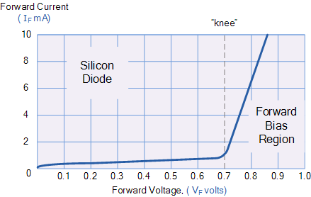
The application of a forward biasing voltage on the junction diode results in the depletion layer becoming very thin and narrow which represents a low impedance path through the junction thereby allowing high currents to flow. The point at which this sudden increase in current takes place is represented on the static I-V characteristics curve above as the “knee” point.
CGPCS Notes brings Prelims and Mains programs for CGPCS Prelims and CGPCS Mains Exam preparation. Various Programs initiated by CGPCS Notes are as follows:-